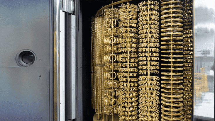
Atomic layer deposition (ALD) is a critical technique in semiconductor manufacturing, valued for its ability to produce ultrathin, conformal films with atomic-scale precision. However, the inherently surface-sensitive nature of ALD makes it highly vulnerable to contamination, which can severely degrade film quality, device performance, and yield. The semiconductor industry, through SEMI standards and best practices, places strong emphasis on minimizing contamination across all stages of the ALD process.
Contamination in ALD arises from multiple sources. Particulate matter, originating from reactor walls, gas lines, or wafer handling systems, can create pinholes or roughness in the nanoscale films. Molecular contaminants, including volatile organic compounds and airborne bases, adsorb onto wafer surfaces and interfere with precursor chemisorption, leading to non-uniform growth or unwanted impurities such as carbon and nitrogen. Trace metal contaminants from precursor impurities or reactor corrosion can diffuse into the active device regions, causing electrical defects and reliability failures.
SEMI provides comprehensive guidelines to address these risks. These include stringent specifications for precursor purity, with maximum allowable impurity levels for metals and organics. For example, SEMI standards define acceptable concentrations of sodium, iron, copper, and other metals in liquid and gaseous precursors. Similarly, they recommend cleanroom classifications and environmental controls for ALD tool installation, including humidity, temperature, and airborne molecular contamination limits.
Best practices based on SEMI recommendations include using high-purity stainless steel gas lines with electrophoretic polishing to reduce particle shedding, installing point-of-use purifiers to remove trace moisture and oxygen, and implementing continuous monitoring with particle counters and mass spectrometers. Regular preventive maintenance, such as in-situ plasma cleaning or wet cleaning of reactor chambers, is also recommended to remove accumulated by-products. Furthermore, proper wafer handling with minimized exposure to ambient air and rigorous incoming material inspection complete the contamination control strategy, ensuring high reproducibility and yield in advanced semiconductor fabrication.